Home Top Market Share in Yao/Unique Companies
 Fujiwara Denshi Kogyo Co., Ltd.
Reducing burrs and dust by up to 98% in stamping processes
Fujiwara Denshi Kogyo Co., Ltd.
Stamping of printed circuit boards
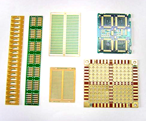
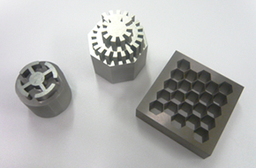
Printed circuit boards are crucial components of cellular phones and home appliances, as well as many other electronic devices. Generally, fiberglass is woven into the material used for printed circuit boards. This material is layered multiple times and then solidified by using a resin. Punching through this material during the stamping process is done using a machine press, which can create fine dust and burrs on the product. Because of this, in the printed circuit board stamping industry, dust contamination and burrs on the printed circuit boards were something that was considered unavoidable.
The SAF processing method developed by Fujiwara Denshi Kogyo has resolved this manufacturing issue.


The SAF processing method
-High-accuracy, low-cost processing technology-
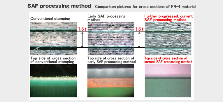
In situations where printed circuit boards were manufactured with a need for high quality, the traditional method has been to employ a secondary process called shaving. This process would cut off the burrs that could cause circuit problems.
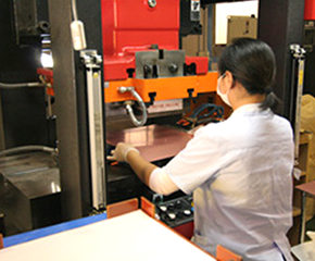
The SAF processing method allows a printed circuit board to be stamped cleanly, as if it was cut with a very sharp blade, thus preventing burrs and dust by up to 98%. This has enabled Fujiwara Denshi Kogyo to perform stamping of high-quality printed circuit boards that are suitable for use in automobiles and other precision equipment at rapid production time and low cost.
The company received orders of printed circuit boards for immobilizers (anti-theft electronic key for automobiles). By utilizing this processing technology, a high market share was secured. This led to the recognition of our high technical capabilities, earning acclaim in the field of board processing used for LEDs, where high accuracy and quality is demanded.

Development of the SAF processing method
-Manufacturing differently from other companies-
Fujiwara was established in 1993, after the collapse of the economic bubble, at a time when domestic printed circuit board processing was moving abroad in order to lower costs, forcing us into a harsh pricing competition. “The situation is never going to change if we keep doing the same thing as the other companies. We need to do something different.” According to this philosophy, company CEO Mr. Fujiwara decided to develop a new technology in 1999.
“If we finish our products cleanly and beautifully, our customers will be pleased.” This simple idea kick-started the development of methods to prevent burrs and dust contamination in stamping printed circuit boards. After 5 years and significant research and development, the SAF processing method was created, providing the company with a competitive edge and creating a high level of added value to customers through making high quality available at a low cost.

Super SAF processing method
“No burrs, no dust contamination” -Setting a new goal: The Super SAF processing method-
We are going to continue working to improve our methods to achieve the goal of “creating something completely new in the manufacturing world” of stamping and processing. Never content to rest on past successes, Fujiwara is doing research every day in order to develop the Super SAF processing method, an enhanced version of the burr- and dust-free SAF processing method.
- Fujiwara Denshi Kogyo Co., Ltd.
- ○Address: 2-51, Minamikinomoto, Yao Ciry, Osaka 581-0042, Japan
- ○TEL: +81-(0)72-991-3927
- ○FAX: +81-(0)72-991-3996
- ○Homepage: http://www.fdk-ltd.jp


